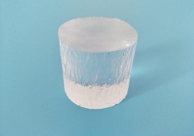
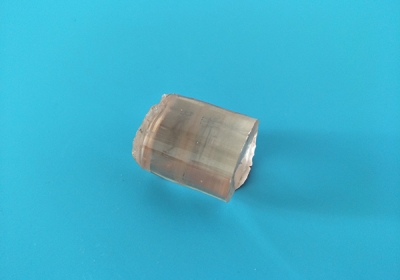
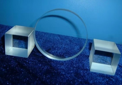
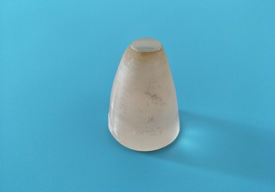
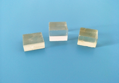
Ge

| Product name | Ge | ||
| Product introduction | The chemical symbol is Ge, which is mainly used for making semiconductor devices, infrared optical devices, solar cell substrates and other materials. | ||
| Technical parameter | Density | 5.765g/cm³ | |
| Melting Point | 937.4℃ | ||
| Thermal Conductivity | 640 | ||
| Doped Material | No doped, Sb-doped, In/Ge-doped | ||
| Type | /;N;P; | ||
| Resistivity (W.cm) | >35;0.05;0.05-0.1 | ||
| EPD | <4x10³/cm2<4x103/cm2<4x103/cm2 | ||
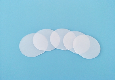
| Regular size | Crystal Orientation | <111>,<100>and<110>±0.5o | |
| Standard Polishing Dimension (special size can be customized according to customer needs) | Φ1”x 0.3mm; Φ2”x 0.5mm (<110> Ra<5A , not polish) | ||
| Note: Substrates with special dimensions and directions can also be provided according to customer requirements | |||
| Remarks | 1000 class super clean room 100 class super clean bag single piece box or 25 piece plug box packaging | ||
Website of this article:http://www.longsee-laser.com/en/crystalline/37.html